
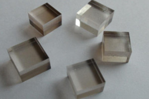
Diamond is considered the hardest substance in the world, which gives it an important role in industry, such as for cutting, grinding, etc. Similarly, in new application fields, diamond is still very good and has huge application potential in high-frequency and high-power devices, optical windows, high-energy particle detectors, quantum information, biosensors and other fields. Especially with the development of the microelectronics industry, after experiencing the first generation of semiconductor materials germanium and silicon, the second generation of semiconductor materials InP and GaAs, and the third generation of semiconductor materials SiC and GaN, people have gradually focused their attention on semiconductors with greater tolerance. On ultra-wide bandgap semiconductor materials such as gallium oxide, diamond, and aluminum nitride, diamond semiconducting materials are shining brightly in the field of conductor devices.
Semiconducting properties of diamond
Diamond is an ultra-wide bandgap semiconductor material with a bandgap width of 5.5 eV, which is larger than wide bandgap semiconductor materials such as GaN and SiC. As shown in the table below, the bandgap width of diamond is 5 times that of Si; the carrier mobility is also 3 times that of Si material. Theoretically, the carrier mobility of diamond is higher than that of existing wide bandgap semiconductor materials (GaN, SiC) It is also more than 2 times higher. At the same time, diamond has an extremely low intrinsic carrier concentration at room temperature. In addition to the highest hardness, diamond also has the highest thermal conductivity among semiconductor materials, which is 7.5 times that of AlN. Therefore, diamond is also called the "ultimate semiconductor" material in the industry. It has shown great application potential in the fields of high-frequency, high-power, high-temperature electronic devices, nuclear radiation detectors, optoelectronic devices, micro-electromechanical systems (MEMS) and other fields. It is these shining points that make it stand out among many semiconductor device materials.
Summary of properties of diamond and other semiconductor materials
| Materials | Bandgap width ev | electron mobility m 2/(V·s) | electron saturation speed 10^7 cm/s | Breakdown field strength | Thermal conductivity W/cmK |
| Diamond | 5.47 | 4500 | 1.5 | >20 | 22 |
| AIN | 6.2 | 1100 | 2.2 | 12 | 2.9 |
| Ga2O3 | 4.8-5.0 | 300 | -- | 8 | 0.11/0.27 |
| GaN | 3.4 | 2000 | 2.5 | 3.3 | 1.3 |
| SiC | 3.3 | 950 | 2.0 | 3.0 | 4.9 |
| GaAs | 1.4 | 8500 | 2.0 | 0.4 | 0.43 |
| Si | 1.1 | 1500 | 1.0 | 0.3 | 1.5 |
Characteristics of diamond as a fourth-generation semiconductor
1. Ultra-wide band gap, ultra-high breakdown field strength, high electron and hole mobility;
2. Acoustically, it has the highest surface acoustic wave speed;
3. Optically, it can transmit photons with energy less than the band gap from far infrared to ultraviolet;
4. In thermal terms, the thermal conductivity exceeds that of copper, and it has the potential for cross-field applications.
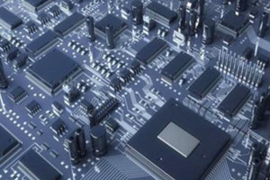
Applications of diamond wafers in the semiconductor industry
Applications: supercomputers, advanced radar and telecommunications systems, ultra-efficient hybrid vehicles, electronics in extreme environments, and next-generation aerospace electronics.
Features: n-type doping technology, large-size and high-quality single crystal, high flatness, high uniformity material epitaxial technology, higher power.
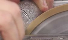
Moresuperhard offers resin diamond cutting discs and metal diamond cutting discs specifically for cutting in the glass industry. It can be used to cut glass optical devices such as quartz glass, K9 glass, coated glass, etc. It can also be used to cut various glass tubes, glass spouts, high borosilicate glass tubes, capillary glass tubes, quartz glass, and crystallized glass.
Polyetheretherketone PEEK has excellent comprehensive properties and can replace traditional materials such as metals and ceramics in many special fields. Moresuperhard has developed targeted grinding wheel formulas for the grinding of special engineering plastics such as PEEK, mainly electroplated grinding wheels, divided into rough grinding and fine grinding.
Add: Zhongyuan Rd, Zhongyuan District, Zhengzhou, 450001, Henan, China
Tel: +86 17700605088