
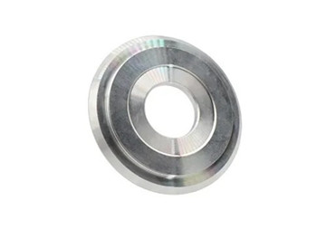
Wafers are the basic raw materials for the production of semiconductor devices. High-purity semiconductor materials are made into wafers through process flows such as crystal pulling and slicing. The wafers are produced through a series of semiconductor manufacturing processes to produce tiny control circuit structures, and then cut , Packaging, and testing become chips, which are widely used in various electronic instruments.
Wafer chamfering and round edges usually use curved cutting or internal circular cutting saw blades. The outer edges of the cut wafers are particularly sharp, in order to prevent corner cracks from affecting the hardness of the wafer, or damaging the surface finish and subsequent processes Because of environmental pollution, special numerical control equipment is required to automatically correct the edge, shape and outer diameter of the wafer. Therefore, the cutting tool directly affects the quality of the finished product.
The production of wafer cutting tools is first roughed by carbide tools, then semi-finished by PCD blades, and finally finished by MKD turning tools to achieve extremely high dimensional accuracy and surface finish.
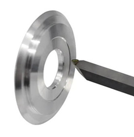
The More super hard turning tool finishes the surface and inner hole of the wafer cutting tool, and the cutting performance is more stable, thereby improving the cutting quality and cutting accuracy of the substrate after the cutting tool is packaged, and greatly increasing the production capacity, tailored to meet the needs of users Its process and project requirements.
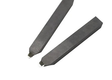
Single crystal tools have many advantages in ultra-precision machining. High hardness and wear resistance can greatly avoid the impact of tool tip wear on workpiece size during ultra-precision machining. In addition, the good thermal conductivity and low thermal expansion coefficient can prevent large thermal deformation during cutting. In addition, the surface roughness of the single crystal tool is relatively small, and the cutting edge is very sharp, reaching Ra0.01-0.006μm, and the single crystal cutting allowance is less than 0.02mm.
Single crystal processable materials and applicable industries are as follows:
1.Metal materials: aluminum alloy, aluminum, brass, copper, gold, nickel, silver, tin, zinc, HRC50 hard steel, etc.;
2.Polymer materials: acrylic resin, nylon, polypropylene, polystyrene, silica gel, etc.;
3.Infrared crystal materials: calcium fluoride, gallium arsenide, germanium, magnesium fluoride, silicon, zinc selenide, zinc sulfide, etc.
4.Military industry: off-axis three-mirror, missile fairing, precise infrared optical system, etc.;
5.Civil: spherical, aspherical free-form lens, Fresnel lens, high-precision mold core, super bright and super uniform light guide plate, compound eye structure, etc.

Learn the technical characteristics, advantages, disadvantages and applicable working conditions of standard TSP and nickel-based coated TSP. Compare their performance differences and master the selection skills for drilling, cutting and grinding scenarios.

With tungsten carbide prices soaring 200%+, PCD & CBN become cost-effective alternatives. Moresuperhard provides high-quality PCD/CBN blanks, grinding wheels & grinders to help manufacturers reduce costs and improve efficiency.
Add: Zhongyuan Rd, Zhongyuan District, Zhengzhou, 450001, Henan, China
Tel: +86 17700605088