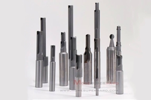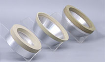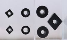
PCD tools for Graphite precision turning
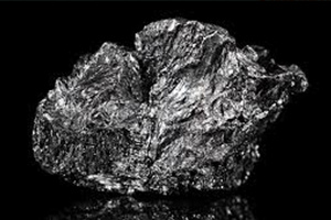
Graphite is an allotrope of carbon. With the rapid development of mold industry, graphite has become an ideal material for mold making with its good physical and chemical properties. Graphite is widely used in refractory materials, conductive materials, wear-resistant materials, lubricants, high temperature resistant sealing materials, corrosion resistant materials, insulation materials, adsorption materials, friction material, and radiation protection materials, these materials are widely used in metallurgy, oil chemical industry, machinery industry, electronic industry, photovoltaic industry, nuclear industry and national defense, etc.
The manufacture of solar cells requires six processes: making wool, diffusion, etching, coating, screen printing and sintering. In one of the processes, plasma-enhanced chemical vapor deposition is used to coat the silicon nitride film on the front of the silicon wafer to reduce the reflection of sunlight and to passivate the silicon wafer surface.

When the cell is processed, the graphite workpiece requires very high size accuracy. The position and size of the workpiece will affect whether the coating film of the silicon chip is uniform. Therefore, for the graphite workpiece with smaller shielding area and more stable and stable silicon chip, the photoelectric conversion efficiency of the battery can be improved.
“More Super Hard” PCD tool can precise turning on graphite workpiece with the diameter of about 15mm, finish shaping the workpiece in one-time, and the dimensional tolerance is under 0.01mm, which can meet different chamfering angles of different types of workpiece. Under the suitable machine conditions and processing parameters, the working life can reach 30,000-40,000 pieces, which is twice as long as competitor’s cutting tool. In addition, compared with other material tools, PCD tool has higher processing efficiency in graphite processing, it reduces the time cost, is an ideal processing scheme.
The graphite processed by “More Super Hard” PCD tool, can be used to fix the silicon wafer, minimize the shielding area, guarantee the photoelectric conversion efficiency of the battery, and further improve the advantages of your product.
<< Prev Article:Polycrystalline diamond (PCD) tool for automotive piston
<< Next Article:Why PCD tools are not suitable for rough processing?
LATEST NEWS
-
20 August 2020
PCD tools grinding wheel
Vitrified bond diamond grinding wheels possess pretty high a...
-
07 May 2020
Precision hole machining
Our company mainly develops a new making holes’ method for P...
CONTACT US
Add: Zhongyuan Rd, Zhongyuan District, Zhengzhou, 450001, Henan, China
Tel: +86 15617330220

