
The dicing blade used in wafer cutting is a missing link in China's semiconductor packaging industry chain, which has been dependent on import for a very long time. No matter from the perspective of national development strategy or national security strategy, this gap must be filled as soon as possible. We should commit to building a production base for wafer cutters in China, realizing the localization of wafer blades, and fully meeting the urgent needs of China's integrated circuit, discrete devices, LED and other industries for dicing blades.
What is Wafer Dicing Blade?
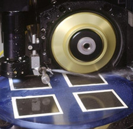
In the early stage of semiconductor wafer packaging, dicing blade is an important tool used to cut wafers and manufacture chips. It has a direct impact on the quality and life of chips. The application of the dicing blade in semiconductor packaging process is shown in the following figure:
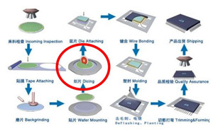
Wafer Dicing
Dicing is commonly used to separate optical components or electronics imaged onto wafers. The substrates can be waxed onto hard mounts to minimize chipping.

What is Wafer Dicing?
The wafer dicing process separates small blocks of semiconducting material (known as dice) from a semiconductor wafer. Depending on the application’s needs, the dicing process may involve wafer scribing, through cutting, or wax mounting. The wafer is sawed in the extra spaces between dice to separate them.
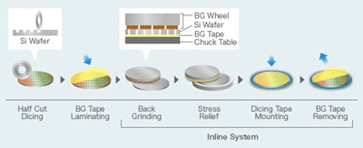
Usually, manufacturers mount wafers onto tape to improve their backside support. Once the wafer has been mounted, it’s loaded into a cassette and then into the actual dicing mechanism, which cuts the wafer into individual dice.
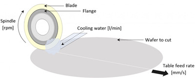
The dicing mechanism contains an abrasive blade that it rotates with a spindle at high speeds (usually 30,000–60,000 rpm).
Blades used for this purpose comprise diamond grit embedded into an electroplated nickel matrix. Because these blades are so strong, they easily crush wafers, and any debris that it creates can be removed while the machine works.
The blade moves between active areas of the dice through dedicated lines known as streets. This creates a groove in the substrate material.
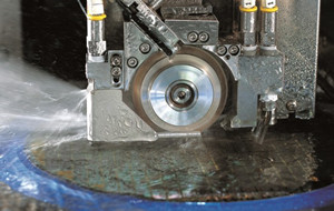
With the miniaturization, high capacity and high efficiency of chips, the structure of chips becomes more and more complex, and the effective space between chips becomes smaller and smaller, so the space of cutting becomes narrower and narrower. This is more and more demanding for precision wafer dicing blades.
At present, there are two ways to cut wafers: one is laser cutting, the other is mechanical cutting, that is, dicing blade cutting. The latter is currently the main force in wafer cutting. The reason for this is that (1) high-power laser cutting can’t use lest produce heat affected zone (HAZ) chip, (2) laser cutting equipment is very expensive (generally in $1 million/table above), (3) laser cutting can't do it all at one time (because the HAZ problem), and thus a second cut still should use dicing blade to finishing, so dicing blade is one of the indispensable material in semiconductor packaging technology.
Most of the silicon substrate integrated circuits and device products need to be cut with a dicing blade when they are packaged. Global economic and semiconductor industry statistics for the past 25 years show that the annual growth rate of the semiconductor integrated circuits and devices market is in line with the annual growth rate of global GDP, so the demand for dicing blades is also increasing year by year.
Analysis on The Market of Dicing Blades:
At present, there are about 10 major manufacturers in the global dicing blades market, leading manufacturers in the industry are DISCO in Japan, ADT in Israel, K&S in the United States, etc. Currently, the domestic annual demand of dicing blades is 6-8 million pieces. According to the estimated price of 160 yuan/piece, the market scale is about 1-1.5 billion yuan. DISCO is basically a monopoly of the domestic dicing blades market. The technical barrier is product’s yield, which, according to DISCO's annual report, is as high as 52% gross margin.
DISCO was founded in 1937 and is headquartered in Tokyo, Japan. Mainly for the manufacture and sales of precision processing equipment and tools, including dicing machine, grinding machine, Surface Planer, polishing machine, etc. The leasing of precision processing equipment and the sale of used equipment, as well as the processing services of precision parts; Mainly used in semiconductors, electronics and construction industry.
Advanced Dicing Technologies (ADT), Israel specializes in semiconductor wafer cutting (dicing), chip packaging cutting (dicing) and microelectronic component related systems, process development and blade manufacturing (Hubless Blades), providing professional dicing and slotting services for electronic and optical devices. In 2003, the investor acquired Kulicke&Soffa (K&S) cutting equipment (dicing machine) and blade manufacturing (Hubless Blades (Sofas) sales department of Kulicke&Soffa Semiconductor Limited (K&S) and established Advanced Dicing Technologies (ADT) Israel. ADT's corporate headquarters, research and development facilities and two production plants are located in Israel. The company employs about 160 professionals.
Kulicke & Soffa, founded in 1951, is a wholly owned American company and a world leader in semiconductor packaging. We have been working with leading semiconductor manufacturers worldwide for many years and have made key contributions to many significant technological breakthroughs in the industry. Kulicke & Soffa is a global leader in semiconductor packaging and electronic assembly solutions for automotive, consumer electronics, communications, computers and industry

All these three have their own leading edge in wafer dicing blades. And we depends on our own scratcher technology accumulation, will open up a new space in this field.
Our dicing blades have the advantages of optimized blade structure, high dicing precision, continuous dicing at high speed, stable performance and long service life, etc., and are able to analyze the size and morphology of diamond particles.
Through scientific and reasonable screening, the concentration, uniformity and concentration of diamond on the blade are optimized. Meanwhile, the innovative process of nickel-based bonding agent is carried out, which can slot and cut all kinds of hard and brittle non-metallic materials. Compared with similar foreign products, it has a very high cost performance.
How to break through?
Wafer dicing blade products, especially the nanoscale wafer dicing blade products for processing thin (below 100μm), ultra small (150 x 150μm below, for example), super crisp (such as Low - K wafers), super numerous nearly 10 layer (such as dielectric layer structure) of the metal layer and the corresponding characteristics of wafer, asked the dicing blade made of every working procedure and process is not only strict, and requires a series of related technology.
The Ni-base blade has a nickel base thickness of 10μm, one-ninth the diameter of an average Asian hair. Therefore, this project adopts a variety of technologies to produce nano-nickel bonding scratcher.
Machining micron level blade. In machining, this project adopts high-precision machining technology to strictly control the concentricity, roundness, parallelism, flatness and surface roughness of the cutter wheel hub.
Measurement error achieve an ultramicrometer level. The internal stress control of nickel - based edge is the most important technical link, which requires special detection means and specially customized equipment to be used in the "constant temperature and humidity" clean room.
At present, some wafers are only about 100μm thick, and the physical characteristics of silica-based chips are very fragile, finishing such wafers, the general blade is unable to meet the dicing quality requirements. The dicing quality criteria are chip integrity, no micro-cracks, no peeling of interfaces, no burrs on the edge of the chip, no cracks on the back boundary, no corners falling off, etc., all of which are measured in micron scale..
Ordinary blades are difficult to meet the technical requirements of cutting wafers based on nickel, so it is more and more important to develop a kind of high performance blade. At present, in the field of dicing blades manufacturing, Disco dominates the market. Several domestic enterprises have been engaged in the research and development of dicing blades for many years, but still have not achieved a breakthrough. This will be the opportunity for our wafer dicing blade project, which will be well positioned in light of the semiconductor industry trends as a whole.
At the beginning of the project, we will mainly produce all kinds of wafer cutters with the biggest and urgent demand in China market then develop special ones. The specific steps are as follows:
1. Si Dicing Blades: for dicing Si-wafers
2. Bevel Dicing Blades: specially for back-cutting
3. GaAs Dicing Blades: specially for dicing GaAs series wafers
4. Low-K Dicing blades: for Dicing Low-k Type Wafers
5. BGA Dicing Blades: for BGA packages
Moresuperhard can provide ultra - thin ( hub type and hubless type) diamond dicing blade for scribing silicon wafers, compound semiconductor wafers (GaAs, Gap), oxide wafers (LiTaO3), glass, crystal, quart, LiTaO3,optical, magnetic material,PCB, Ceramic, BGA, CSP and QFN packages.

PCD tools offer excellent hardness and wear resistance for machining difficult materials, but grinding them poses unique challenges. This article explores common issues such as chipping, high surface roughness, dimensional deviations, burning, and grinding wheel wear. Learn practical solutions to optimize grinding parameters, wheel selection, and machine accuracy to improve tool life and reduce costs.
Discover how our 3A1 ceramic diamond wheel helped a client achieve ultra-precise PCD reamer grinding. Learn how adjusting bond hardness and grit size resolved issues with carbide shank grinding for better edge quality and stability.
Add: Zhongyuan Rd, Zhongyuan District, Zhengzhou, 450001, Henan, China
Tel: +86 17700605088